
Common PCB Assembly Problems (and How to Prevent Them)
Common PCB Assembly Problems (and How to Prevent Them)
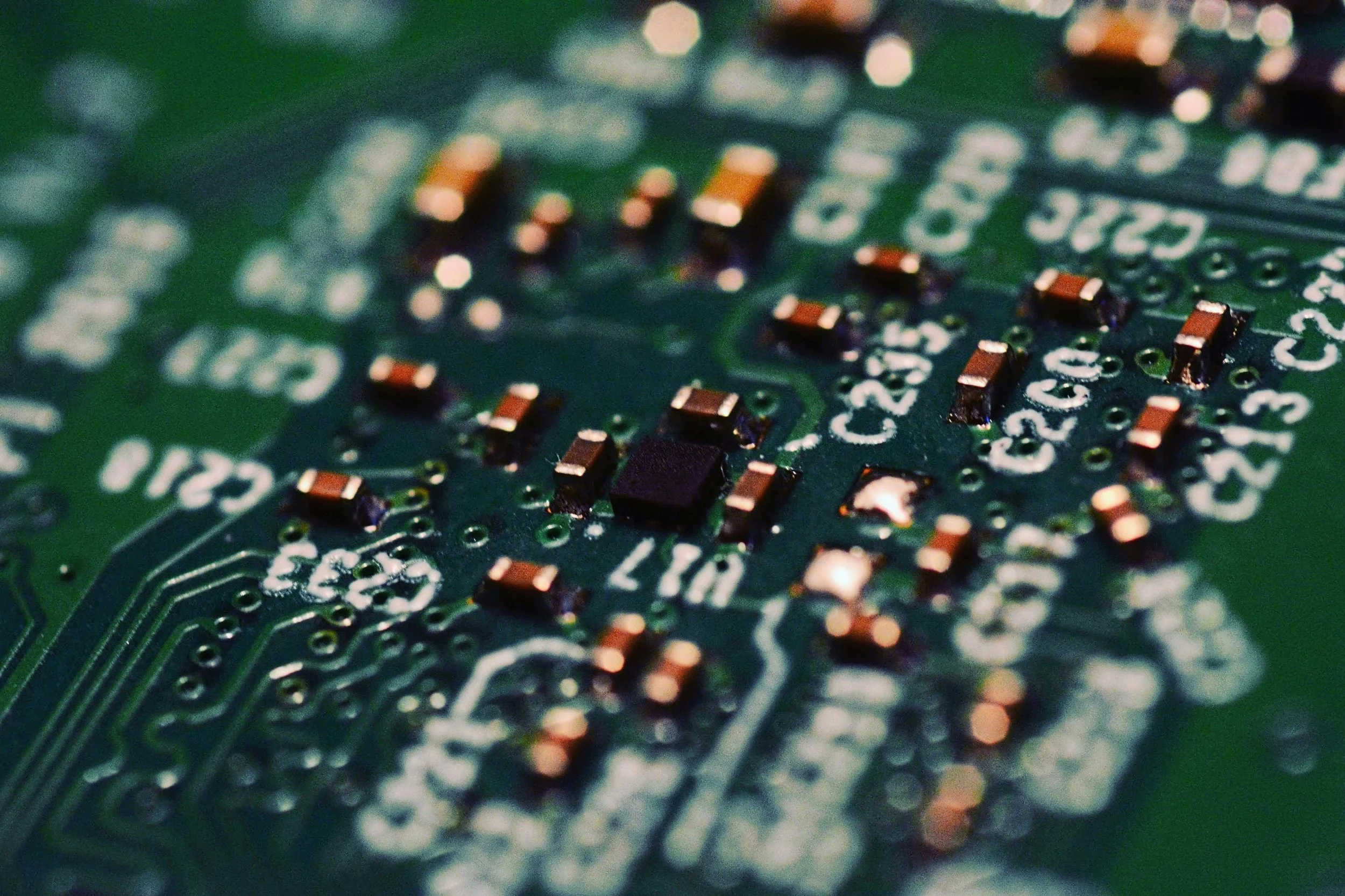
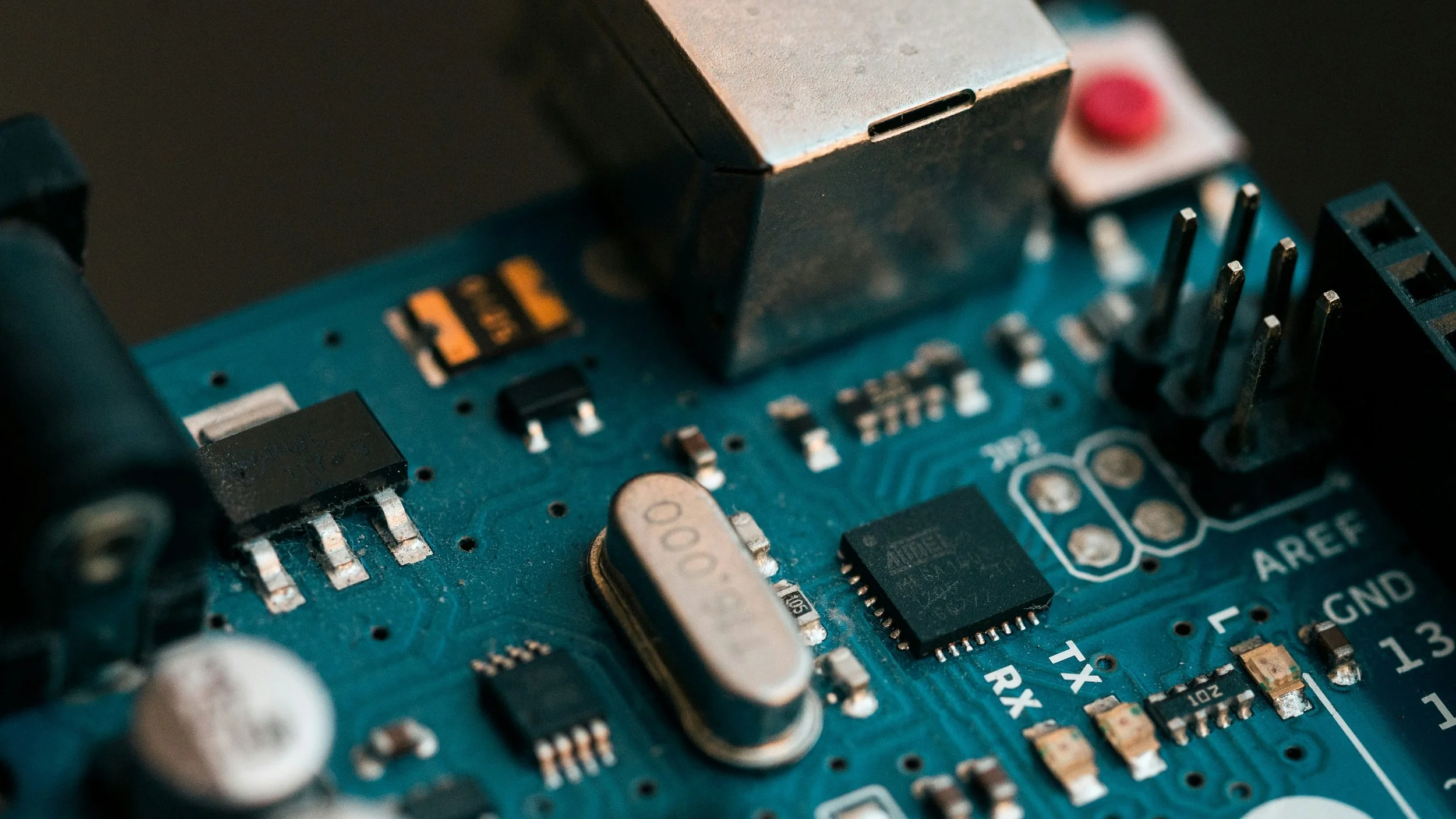
Even with modern manufacturing equipment, PCB assembly can face challenges if the design, files or components are not prepared correctly. Understanding common issues helps engineers and designers prevent costly delays, improve quality and achieve more reliable end products.
Here are the most frequent PCB assembly problems and what you can do to avoid them.
1. Solder Bridges
Solder bridges occur when excessive solder connects two pads that should not be joined.
Causes
Too much solder paste
Poor stencil design
Fine-pitch components placed too close
Prevention
Use correct stencil thickness
Follow IPC-recommended pad spacing
Request a DFM review before manufacturing
2. Tombstoning
This happens when one end of a small component lifts during reflow, causing it to stand upright like a tombstone.
Causes
Uneven heating
Asymmetrical pad design
Misaligned solder paste
Prevention
Ensure symmetrical pad sizes
Use high-quality solder paste
Adjust reflow temperature profiles
3. Misaligned Components
Misalignment can result in poor connections, improper performance or assembly failure.
Causes
Inaccurate placement data
Poorly prepared pick-and-place files
Component packaging issues
Prevention
Provide accurate placement files
Verify footprints match manufacturer datasheets
Use quality component reels/tapes
4. Insufficient Solder Joints
Weak solder joints cause intermittent faults and long-term reliability issues.
Causes
Low paste volume
Oxidised component leads
Incorrect reflow settings
Prevention
Review stencil design
Use fresh components from reputable suppliers
Ensure correct reflow temperature curves
5. Component Polarity Errors
Incorrectly placed polarised components can lead to total board failure.
Causes
Inconsistent silkscreen markings
Ambiguous footprints
Human error during manual placement
Prevention
Double-check polarity on both PCB and BOM
Ensure clear silkscreen markings
Use AOI to verify orientation
6. PCB Warping
Warping affects alignment, solder joint quality and mechanical fit.
Causes
High-temperature processes
Large panel sizes
Thin PCB material
Prevention
Select correct PCB thickness
Use proper panel support in reflow
Consider reinforced materials for large boards
How to Reduce PCB Assembly Problems
Here’s how manufacturers like First Choice Assembly minimise defects:
Thorough DFM reviews
Automated Optical Inspection (AOI)
Controlled reflow profiles
High-quality stencil production
Reliable sourcing for components
Skilled manual finishing for THT assemblies
Improve Your PCB Assembly Quality Today
If you want help reviewing your design, preparing your files or improving assembly yields, our team is ready to assist.
Visit our PCB Assembly page or request a fast quote.