
From Prototype to Production: Mastering the PCB Assembly Lifecycle
For every design engineer, the ultimate goal is a product that not only functions perfectly in the lab but can be manufactured repeatably, affordably, and reliably at scale. The critical juncture where design meets manufacturing reality is the PCB Assembly lifecycle.
Too often, brilliant prototypes fail when they are introduced to the pressures of high-volume production. This "Prototype Gap" is usually the result of a single, overlooked factor: a lack of collaboration with the assembly partner during the initial design phase.
At First Choice Assembly, we view ourselves as an extension of your R&D team. Our lifecycle management approach is structured to catch flaws before they become expensive failures, transforming your design files into market-ready products with maximum efficiency and minimal risk.
The Essential First Step: Design for Manufacture (DFM)
The most valuable service a contract manufacturer can offer is not the soldering itself, but the technical consultancy that precedes it. This process is called Design for Manufacture (DFM), and it is the foundation of quality.
Before a single component is procured or a stencil is ordered, our engineers undertake a rigorous review of your Gerber files and Bill of Materials (BOM). The purpose of DFM is simple: to ensure your board can be built correctly, quickly, and consistently by an automated machine and human team.
A proper DFM review catches issues that a simple software check cannot. These issues often relate to the limitations of physics, heat, and component handling.
Common DFM Pitfalls Caught by Experts
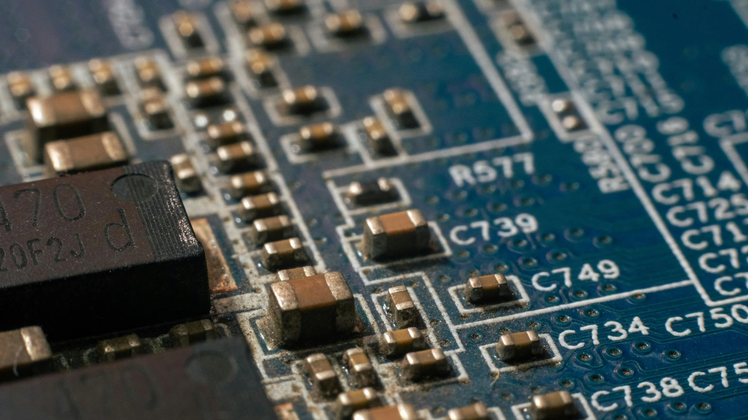
Component Spacing and Placement: Components must have adequate clearance. Incorrect spacing can lead to soldering defects, such as bridging, or make Automated Optical Inspection (AOI) impossible. It also complicates necessary rework later on.
Solder Mask and Pad Geometry: Errors in the solder mask aperture can lead to insufficient paste deposition, causing "tombstoning" or "opens" during reflow. Ensuring correct pad sizes is vital for stable soldering.
Thermal Management: If heat-sensitive parts are placed too close to large thermal masses (like power resistors or transformers), the excessive heat during the reflow process can damage them, leading to premature field failure.
Panelisation Efficiency: For volume production, boards must be arranged efficiently on a panel. A poor panel design wastes material, increases cost, and complicates the singulation (de-panelling) process, introducing mechanical stress into the finished circuit.
By initialising this process early, First Choice Assembly minimises the risk of costly re-spins and ensures that the manufacturing process is optimised before production is green-lit.
Technology Choices: SMT, Through-Hole, and Hybrid Assembly
Modern PCB Assembly relies on two core technologies, and a strategic partner must master both.
Surface Mount Technology (SMT)
SMT is the industry standard for high-density, small-footprint electronic devices. It relies on pick-and-place machines for high-speed, repeatable placement of microscopic components. Our investment in cutting-edge SMT equipment ensures precision placement and controlled reflow soldering, which is critical for complex integrated circuits and fine-pitch components.
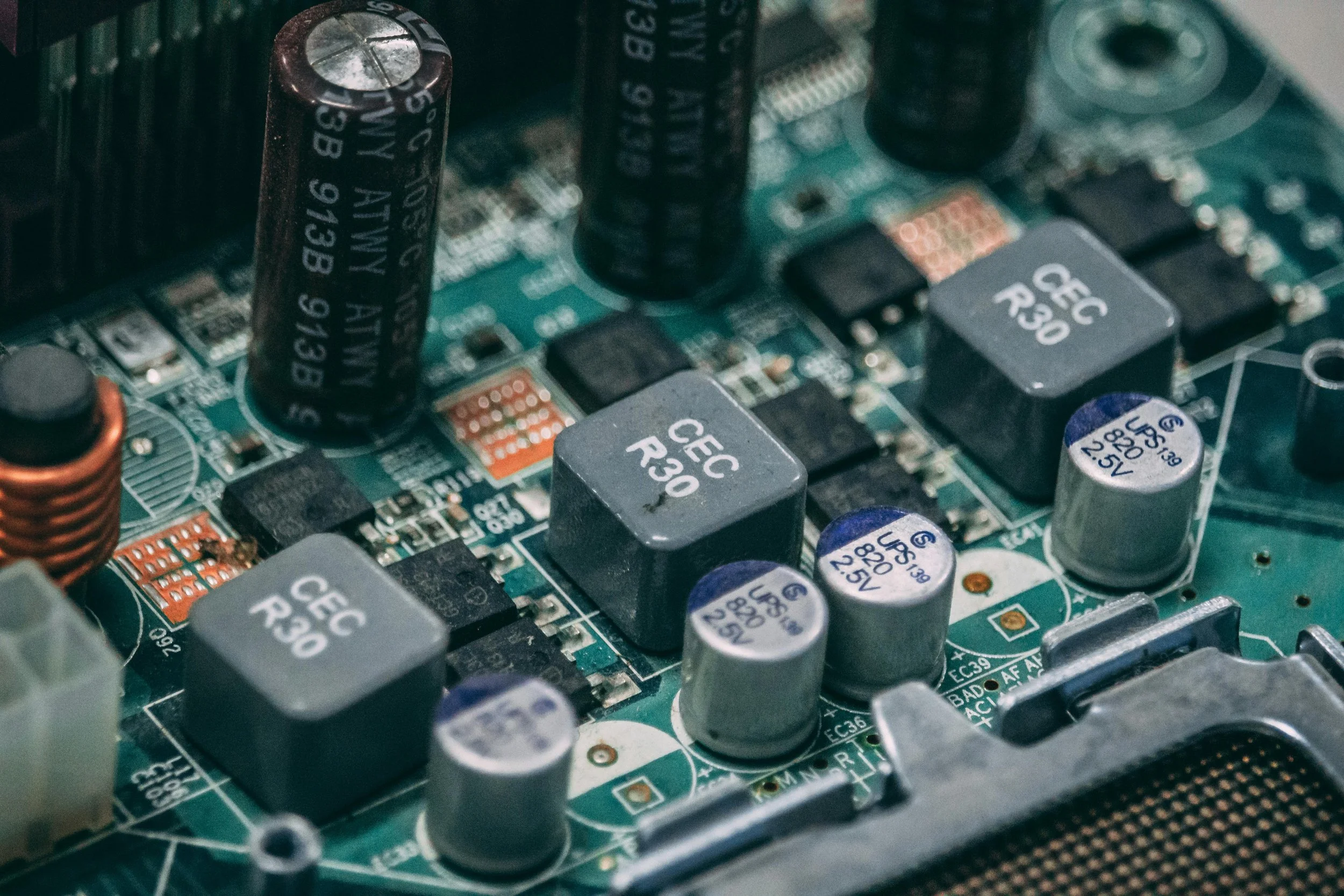
Through-Hole Technology (THT)
THT remains essential for components that require high mechanical strength or need to dissipate large amounts of heat; for example, connectors, large electrolytic capacitors, and high-power inductors. This often requires selective soldering or skilled manual assembly.
The Hybrid Advantage
Most advanced products require both. This is Hybrid PCB Assembly. Many smaller, specialist assemblers struggle to transition seamlessly between these two technologies on the same line. First Choice Assembly is structured to integrate both SMT and THT processes efficiently. This means your board can feature high-density digital circuitry alongside rugged connectors and power components without compromising quality or increasing lead times.
Scaling with Confidence: Consistency and Quality Assurance
A prototype run of ten boards is easy; delivering ten thousand boards that are all functionally identical is the true test of an electronics manufacturing service (EMS) provider.
To guarantee quality across volume, we employ rigorous inspection and testing procedures:
Automated Optical Inspection (AOI): Following the soldering phase, every board passes through our AOI machinery. The AOI system uses high-resolution cameras and programmed algorithms to check every solder joint and component placement against the CAD files. This process is faster and more reliable than human inspection, virtually eliminating errors like missing components, polarity inversions, or insufficient solder.
Functional Circuit Testing (FCT): For many clients, we develop custom test jigs to verify that the final assembled board performs its intended electronic function. This is the ultimate validation, ensuring not just that the components are there, but that the circuit works.
Our internal processes, backed by our ISO 9001:2015 accreditation, define the standards we uphold for quality rigour, full component traceability, and efficient production flows. This focus on a repeatable, documented process is what allows us to confidently offer our Lifetime Assurance on workmanship.
Partnering for Success
Choosing a partner for your PCB Assembly is not simply a procurement decision; it is an engineering decision. You need a team that understands the lifecycle, from the intricacies of DFM to the challenges of scaling production in a consistent and reliable manner.
By partnering with First Choice Assembly, you gain the technical expertise and quality control needed to ensure your design succeeds both on the bench and in the market.
Ready to start your production journey with a partner that builds confidence into every circuit? Get a quote for your next project on our PCB Assembly page.