
How to Design for SMT Assembly: Key Considerations for Better Manufacturing

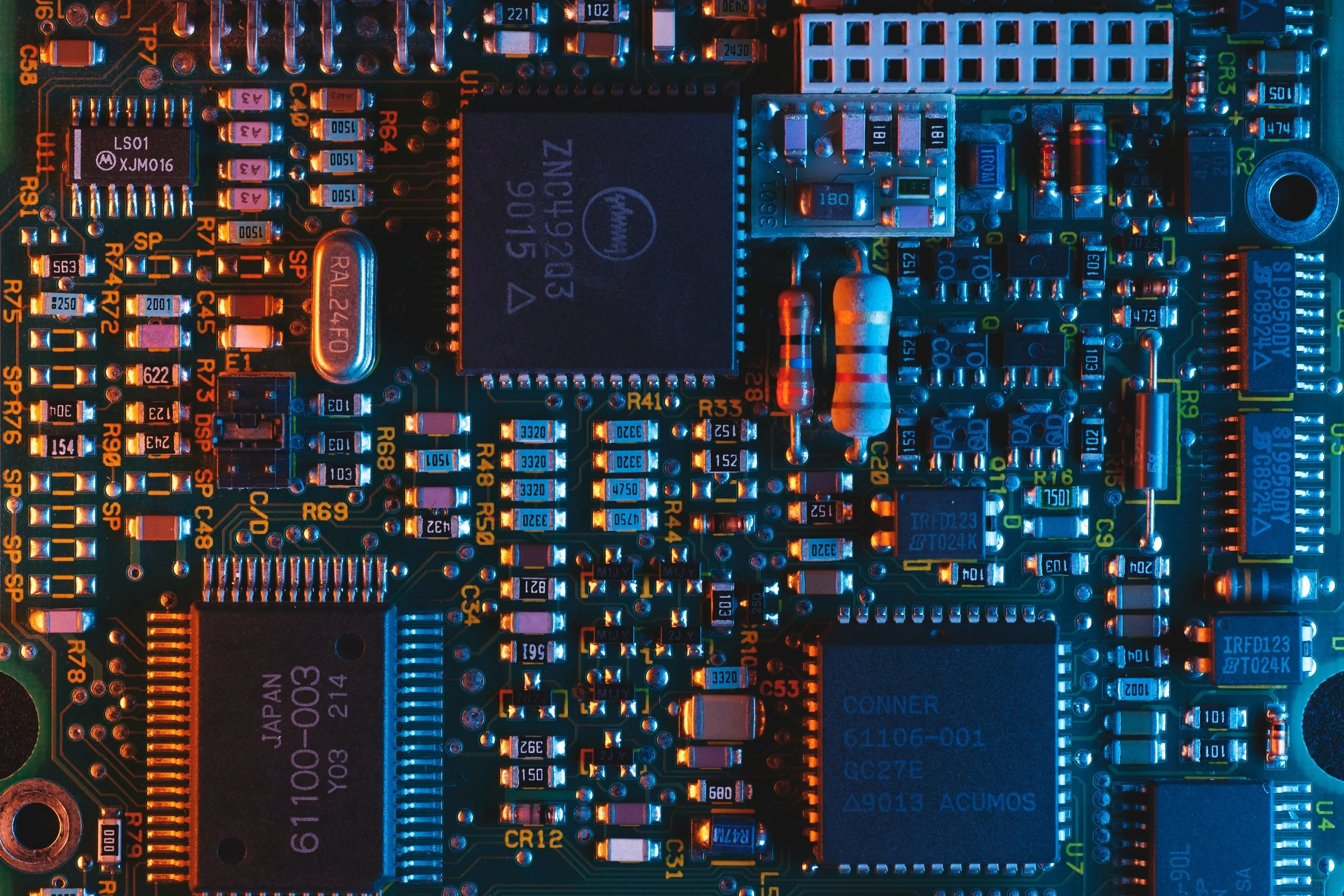
Surface Mount Technology (SMT) is the foundation of modern electronics manufacturing. It enables compact designs, faster production and improved performance. However, even the best concepts can fail if the printed circuit board design is not optimised for assembly.
Designing for SMT assembly is not just about making a circuit work. It is about ensuring your pcb assembly design can be manufactured efficiently, reliably and at scale. Poor design decisions can lead to defects, delays and increased costs.
This guide covers the key considerations for optimising your pcb circuit board design for SMT, combining best practice with real-world manufacturing insight.
What is SMT and Why Design for Manufacture Matters
SMT technology involves mounting components directly onto the surface of a printed circuit board, rather than inserting them through holes. This allows for higher component density and automated assembly.
However, SMT is highly sensitive to design quality. Small inconsistencies in layout, spacing or pad design can result in:
Tombstoning
Solder bridges
Misalignment
Component failure
This is why Design for Manufacture (DFM) is critical. A strong pcb design engineering approach ensures your design works not just electrically, but also in real production environments.
Step-by-Step: How to Design for SMT Assembly
To optimise your smt circuit board assembly, follow a structured approach:
Step 1: Plan Component Placement
Ensure logical grouping, consistent orientation and adequate spacing between components.Step 2: Define Accurate Pad and Footprint Design
Use standardised footprints and ensure compatibility with surface mount device soldering processes.Step 3: Optimise Routing and Trace Widths
Design traces to handle current loads while avoiding unnecessary complexity.Step 4: Apply DFM Principles
Incorporate fiducials, panelisation and test points early in the design.Step 5: Validate for Manufacturing
Review your design with your assembly partner before production to identify potential issues.
This structured approach ensures your pcb design services output is ready for efficient manufacturing.
Component Placement: Optimising for Accuracy and Efficiency
Component placement is one of the most important factors in pcb assembly design.
Best Practices:
Maintain consistent orientation for automated pick-and-place machines
Keep adequate spacing between components to avoid solder bridging
Place smaller components away from large thermal masses
Group related components to simplify assembly and testing
Real-world insight:
A common issue in smt surface mount technology assembly is overcrowded layouts. This makes inspection difficult and increases the risk of defects during reflow.
PCB Trace Widths and Routing Design
Trace design directly impacts both electrical performance and manufacturability.
Key Guidelines:
Use appropriate trace widths based on current requirements
Maintain consistent spacing to reduce interference
Avoid sharp angles in routing
Keep high-speed and sensitive signals properly isolated
Well-designed circuit board patterns reduce production risk and improve long-term reliability.
Pad Design and Surface Mount Device Soldering
Pad design plays a critical role in successful SMT assembly.
Best Practices:
Follow IPC footprint standards
Ensure correct pad size for each component
Maintain consistent solder mask openings
Design pads to support even solder distribution
Common Issues:
Incorrect pad sizing can cause tombstoning
Poor spacing can lead to solder bridging
Uneven paste distribution can cause weak joints
Accurate pad design is essential for reliable surface mount device soldering.
Solder Paste and Stencil Design Considerations
Solder paste application is one of the most overlooked areas in pcb circuit board design.
Key Considerations:
Ensure stencil thickness matches component size
Control paste volume to prevent defects
Use aperture design to improve paste release
Avoid excessive paste on fine-pitch components
Poor solder paste design is a leading cause of defects in smt circuit board assembly.
Thermal Management in SMT PCB Design
Heat distribution can significantly impact assembly quality.
Best Practices:
Balance copper areas across the board
Use thermal relief pads where needed
Avoid placing heat-sensitive components near high-power areas
Design for even heat distribution during reflow
Poor thermal design can lead to warping, delamination and inconsistent solder joints.
Design for Manufacture (DFM): Critical Rules for SMT Assembly
DFM ensures your design is suitable for real-world manufacturing.
Key DFM Elements:
Add fiducial markers for accurate alignment
Design boards for panelisation
Ensure sufficient edge clearance
Include test points for inspection
Real-world insight:
Many delays in pcb assembly occur because designs do not fully consider manufacturing constraints. Addressing DFM early reduces cost and improves production speed.
Pick and Place and Assembly Process Considerations
Designing with the assembly process in mind improves efficiency and reduces errors.
Key Factors:
Component size compatibility with machines
Orientation for automated placement
Avoiding shadowing during soldering
Ensuring accessibility for inspection equipment
Understanding SMT technology from a manufacturing perspective leads to better pcb assembly design outcomes.
Common SMT Design Mistakes to Avoid
Even well-planned designs can fail if key details are overlooked.
Frequent Mistakes:
Components placed too close together
Inconsistent orientation across the board
Missing fiducial markers
Poor pad and footprint design
Ignoring pick-and-place limitations
Real-world insight:
We often see designs that work electrically but fail during assembly due to simple layout issues. These problems can usually be avoided with early design review.
Preparing Your Files for SMT Assembly
Before manufacturing, ensure your design package is complete.
Required Files:
Gerber files
Bill of Materials (BOM)
Pick and place files
Assembly drawings
Using a reliable online circuit board designer or working with experienced pcb design engineering teams helps ensure accuracy and readiness for production.
SMT vs Through-Hole: Design Considerations
While SMT dominates modern electronics, some designs still require through-hole components.
SMT Advantages:
Higher component density
Faster automated assembly
Lower production costs
Through-Hole Considerations:
Stronger mechanical connections
Suitable for high-stress components
Many projects use a hybrid approach, combining both methods for optimal performance.
Real Manufacturing Insight: Designing for Success
Designing for SMT is not just about following guidelines. It is about understanding how designs behave during real production.
In practice, the most common issues we see include:
Designs that do not allow for proper inspection
Inconsistent spacing causing solder defects
Missing manufacturing features such as fiducials
Addressing these early ensures smoother production and better product reliability.
Summary: Key SMT Design Principles
To optimise your printed circuit board design for SMT assembly:
Plan component placement carefully
Use correct pad and footprint design
Optimise trace widths and routing
Apply DFM principles from the start
Design with the assembly process in mind
A well-optimised pcb assembly design reduces defects, lowers costs and improves production efficiency.
FAQs
What is SMT in PCB design?
SMT is a method of mounting components directly onto the surface of a printed circuit board, enabling automated and high-density assembly.
Why is DFM important in SMT?
DFM ensures your design is suitable for manufacturing, reducing defects, costs and production delays.
What causes SMT assembly defects?
Common causes include poor pad design, incorrect solder paste application and inadequate component spacing.
How do you optimise a PCB for SMT assembly?
Optimisation involves proper component placement, accurate pad design, effective routing and applying DFM principles throughout the design process.